We have been hearing about the solar revolution for several years now, whose main mantra is this: A day will come when we will use electricity for free. The main source of this electricity is the sun. Studies have shown that, on a sunny day, the sun radiates about 1000 watts of light energy per square unit area of the earth’s surface! If we could collect all this energy, we would be able to power our homes, offices, and institutions completely.

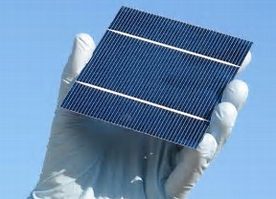
The solar cells we see in calculators or satellites are photovoltaic cells or modules (a module is a collection of cells housed in a single frame that are electrically connected together). “Photo” means light, and “voltaic” means electric. In other words, a photovoltaic cell is a photoelectric cell that converts light energy into electricity.
Photoelectric cells are made of semiconducting materials. Currently, silicon is the most commonly used semiconductor. Essentially, when light strikes these cells, a certain portion of that light is absorbed by the semiconductor. This light energy releases electrons from their atoms, allowing these electrons to move freely. Each photoelectric cell contains one or more electric fields that force these free electrons to move in a particular direction. The flow of these electrons creates an electric current. By attaching metal plates to the top and bottom of the cells, the electricity can be channeled outside.
This is the basic process, but the actual phenomenon is even deeper. Let’s take a closer look at what actually happens with a silicon-based cell.
Silicon has some unique chemical properties. A silicon atom has 14 electrons, arranged in three different energy levels. The two levels closest to the center are completely filled with electrons. The outermost level is half-full, containing 4 electrons. Every silicon atom always wants to fill its outermost shell to achieve 8 electrons. To do this, each silicon atom shares its electrons with four neighboring atoms, creating bonds. Imagine each atom holding four other atoms with four hands. In this manner, a crystalline structure is formed, which is essential for photoelectric cells.
Until now, we have discussed pure silicon crystals. Pure silicon is largely an insulator, as it does not have any free electrons in its natural state. To use this silicon as a solar cell, the silicon crystal needs to be slightly modified.
A solar cell uses impure or “doped” silicon. Impure silicon is made by mixing other atoms with silicon atoms, thereby changing its properties. While we usually consider impurities undesirable, in this case, the impurity actually controls the entire functionality of the cell. In fact, the impurity is intentionally added. For instance, imagine adding one phosphorus atom per million silicon atoms. Phosphorus has 5 electrons in its outermost shell. While four of those electrons bond with adjacent silicon atoms, one electron remains free—not bonded to anything.
When pure silicon gains energy (such as from heat), some electrons break free from their bonds and leave their atoms. Each electron that leaves creates a “hole.” These electrons then move around the silicon crystal, searching for holes to fall into. These electrons are called free carriers, and they conduct electricity. In pure silicon, there are so few of these electrons that they do not play a significant role in electrical conduction. Therefore, pure silicon, in essence, acts as an insulator. However, phosphorus-doped silicon is different. In this case, the extra electrons from phosphorus atoms are easily freed even by a small amount of energy, since they are not involved in any bonds. As a result, compared to pure silicon, doped silicon provides many more carriers for conduction. Mixing impurities with pure silicon is called doping. When phosphorus is added, the resulting doped silicon is called N-type silicon. Here, electrons act as carriers, and since their charge is negative, it is called “n”-type. Thus, we see that doped silicon is a much better conductor than pure silicon.
In reality, one part of a solar cell is N-type. The other part is doped with boron, which is called P-type silicon. Boron has 3 electrons in its outermost shell. As a result, P-type silicon forms extra “holes” instead of extra electrons, which act as charge carriers. The absence of an electron is called a hole, and so the charge of a hole is opposite to that of an electron, meaning it is positive. Since holes have a positive charge, it is called “p”-type. These holes move much like electrons do.
An amazing event occurs when N-type and P-type silicon are brought together. When these two types are joined, an electric field is created at the junction. Without this electric field, a photovoltaic cell simply won’t work. So every photovoltaic cell must have at least one electric field.
Let’s now see what actually happens when N-type and P-type silicon are connected. The free electrons in the N-type region find holes in the P-type region and quickly fill them. As a result, there is a build-up of positive charge on the N-type side of the junction and negative charge on the P-type side. The question may arise: Do all free electrons fill all the holes? No, because an electric field is formed at the junction, oriented so that it acts as a barrier, preventing more electrons from the N-type from moving into the P-type. Eventually, equilibrium is reached when the electric field keeps both sides separated.
Figure 1 – The effect of the electric field in a photovoltaic cell
Next, let’s see what happens when light strikes in this scenario. When photons (particles of light) hit the solar cell, electron-hole pairs are broken apart and electrons are freed. Each photon with enough energy can free one electron, creating a corresponding hole. If this event occurs near the electric field or if the newly created electron and hole wander near the region influenced by the electric field, that field pushes the electron towards the N-type side and the hole towards the P-type side. If an external connection is made, the electrons travel through that path to the P-type area and fall into a hole. This flow of electrons creates electric current, and the cell’s electric field maintains a potential difference. Power is produced by the combination of current and potential difference, equal to their product.
Figure 2 – The functioning of a photovoltaic cell
Now, the question is: How much solar energy can a photovoltaic cell absorb? Unfortunately, the truth is that most cells can absorb only about 25 percent of the total solar energy.
Sunlight contains light of varying wavelengths, each with photons of different energy. Since the photons in the light falling on a solar cell have various energy levels, not all are strong enough to create electron-hole pairs. The photons that are too weak simply pass through the cell without freeing any electrons. Only photons with energy above a certain threshold can free electrons. For crystalline silicon, this threshold is 1.1 eV (electron volts), which we call the band gap energy. If a photon has more energy than this, the excess energy is wasted. In this way, about 70 percent of solar energy is wasted.
Now, you might ask: Why don’t we use materials with even lower band gap energy to harness more photons? Unfortunately, the band gap energy also determines the strength of the electric field created. That is, in cells made from materials with lower band gap energy, the potential difference is so low that it becomes unacceptable. About 1.4 eV is generally considered ideal for solar cells.
Apart from the photon energy wastage in solar cells, there are other losses as well. The electrons flow out of the cell through external connections. The lower part of the cell is covered with metal to improve conductivity. But if the upper part is also completely covered, photons will be blocked by the opaque conductor, and current won’t be generated. That’s why a transparent conductor is used on the top. If we only provide metal contacts on both sides, the electrons have to travel a longer distance to reach those contacts. Since silicon offers more resistance and is not as good a conductor as metals, this longer path is arduous for electrons and leads to increased losses. To minimize these losses, the cell’s surface is covered with a metal grid, so the electrons do not have to travel far.
There is another issue: silicon is a very shiny material, so a significant portion of incident photons are reflected away. For this reason, the upper surface of the cell is coated with an anti-reflective material. Finally, the cells are covered with a glass lid to protect them from contact with other substances. To obtain significant voltage and power, a number of cells (usually 36) are connected as needed to form a PV module. Then, the entire module is covered with a glass lid.
Figure 3 – Structure of a silicon photovoltaic cell
Source: www.howstuffworks.com


underline কেন আসল?
টপিক ইলেক্ট্রনিক্স হবে কিন্তু ফন্ট প্রবলেমের কারণে ধর্ম ও বিজ্ঞান দিয়ে দিয়েছি। কি করতে পারি?
লেখা জমা দেবার পরে লেখকরা (যতবার খুশি) পুনরায় এডিট করতে পারবেন। লগিন করার পরে সদস্য মেনুর পাশে “আপনার প্রবন্ধসমূহ” দেখুন এ তা পুনরায় এডিট করুন। underline হবার কারণ হল আপনি html এ Strong কোডটি ব্যবহার করেছেন, আপনার সোর্সটি দেখুন। বিস্তারিত লেখকদের জন্য ম্যানুয়ালটি দেখুন। টপিক পরিবর্তন করে দিলাম ও underline ঠিক করে দিলাম।
HelpDesk
Biggani.org
অনেক অনেক ধন্যবাদ।
খুব মজার ও গুরুত্বপূর্ণ একটা বিষয় নিয়ে সহজ ভাবে শেখানো হয়েছে ও আগ্রহও সৃষ্টি করা হয়েছে।
ধন্যবাদ।