The Beginning of Nanotechnology
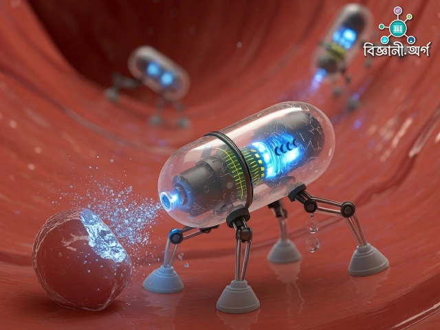
In the 21st century, if there’s any topic as widely discussed as IT, it’s nanotechnology. A significant portion of Japan’s national research budget is dedicated to nanotechnology-related fields. Not only Japan—Europe, America, China, Korea—all these countries are pushing forward with research in this area. Why? Because they all want to be leaders and pioneers in the field. Although America leads in IT, other countries do not want to lag behind in nanotechnology. As a result, there is intense global competition. Why is everyone so interested in nanotechnology? The simple answer is: the future will be the era of nanotechnology. Have a heart disease? A nano-robot will enter your body and repair it. Your wristwatch will become your computer, your mobile—everything. And all this will be possible thanks to nanotechnology.
What is Nanotechnology?

Nano is a unit of measurement. The metric system began in France in 1790. The National Assembly of France formed a committee to standardize units, and they first proposed a decimal (ten-unit) metric system and introduced the unit of length, “meter.” They defined one meter as one forty-millionth part of the Earth’s meridian. The word “meter” comes from the Greek word “metron,” meaning measurement. One hundredth of a meter is called a centimeter, a standardization enacted by law in France in 1793. In 1960, the definition of meter changed—to one 1,650,763.73th of the wavelength of orange radiation from krypton-86. In 1983, the definition changed again: now, one meter is the distance light travels in a vacuum in 1/299,792,458th of a second. One billionth (1,000,000,000th) of a meter is called a nanometer. The word “nano” comes from the Greek “nanos,” meaning dwarf, though it is used as a unit of measurement. Technologies related to this nanometer scale are referred to as nanotechnology.
The meter is a unit deeply integrated into our daily lives. We measure our houses, furniture, everything in meters. Until World War II, the precision of instruments was measured on the millimeter scale. There was little thought beyond the millimeter. But after WWII, a new era in science and technology began. Semiconductors began their journey, starting with the invention of the transistor. At that point, we began to think in terms of micrometers—the start of microtechnology.
Then technology accelerated at a tremendous pace. Consumer products like televisions, radios, fridges, etc.—the race began to make these smaller and smaller. Companies competed to deliver the smallest possible products to consumers. The advancement of semiconductor technology made this possible. When we look at the size of early radios or TVs today, we laugh—how could people use such large devices? But now, ultra-thin televisions are available for wall mounting like calendars, and even smaller ones are coming.
In 1980, IBM researchers invented the STM (Scanning Tunneling Microscope), a device capable of visualizing structures down to the atomic level. This invention made nanotechnology a practical reality. How does the STM work? The device has an extremely fine needle-like tip. When brought very close to a conductive material, a minuscule amount of electric current called “tunneling” flows. The amount of this current is used to create an image of the material’s surface atoms. However, the sample must be conductive to be imaged with STM. So, how to visualize non-conductive atoms? Human ingenuity prevailed—as always—using AFM (Atomic Force Microscope). STM works with tunneling electricity, while AFM uses a fine needle to scan atomic structures.
Top-Down and Bottom-Up:
There are two approaches in nanotechnology. One is from top to bottom (Top-Down), and the other is from bottom to top (Bottom-Up). In the top-down method, something large is cut down to a specific, small shape, usually through an etching process. Bottom-up, on the other hand, builds larger objects from tiny components. Our current electronics use top-down technology, while nanotechnology relies on the bottom-up technique—creating things from nanometer-scale elements. For easier understanding, imagine you need a specific type of DNA. In the bottom-up process, you assemble small components to create the desired DNA. However, nanotechnology isn’t limited to only bottom-up techniques—often, both top-down and bottom-up methods are combined.
Computer users know that computer prices drop every year, and each year you can get more power for less money. This is also due to nanotechnology. The processor inside a computer—most of you have heard of Intel processors—contains countless extremely small, nanometer-scale circuits, built using nanotechnology. In Intel processors, circuits are patterned on silicon, currently at a size of 100 nanometers. Within the next three years, this will shrink to 70 nanometers, and in seven years, to 50 nanometers. Intel hopes that by 2010, they will reach 30 nanometers, halving the processor’s size from today. The day is not far when your mobile device will perform like a computer (in fact, such mobile devices already exist now). Similarly, computer hard disks are increasing in storage capacity each day, thanks to nanotechnology—the 300-gigabyte hard drive now available would have been unimaginable just 10 years ago.
The Ghost of Static Electricity
Building circuits with nanotechnology isn’t as simple as it may seem. The main barrier is static electricity. Have you ever come in from outside on a cold day and touched a doorknob, receiving a shock? Or tried to take off a sweater in the dark and seen sparks? These are daily examples of static electricity. Conventional electrical circuits are protected against static electricity, or they would be destroyed by it. But in nanotechnology, electrical circuits are so unimaginably small that traditional protection methods don’t work. Scientists are studying how to protect these circuits at the nanoscale. How does static electricity damage circuits? In tiny circuits, static electricity can produce temperatures up to 1,500°C—enough to melt the materials and destroy the circuit. That’s why since 1997, copper has replaced aluminum in IC circuits—copper has a melting point of 1,083°C, compared to 660°C for aluminum, making copper more robust at high temperatures.
A Look Back at the Beginning:
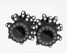
November 9, 1989, is perhaps one of the most significant milestones for nanotechnology. On this day, at IBM’s Almaden Research Center in California, Don Eigler and Erhard Schweizer created the IBM logo using 35 xenon atoms. For the first time, humans could manipulate atoms to create something by design. This day may be marked as the first milestone in nanotechnology history. It was the day humans managed to alter the most fundamental structures of nature—the atom. By creating atomic structures at will, endless possibilities opened up. For example, the difference in atomic structure alone makes coal cheap and diamond expensive. Both are made of carbon, but diamond’s structure makes it the hardest substance on earth, while coal or pencil graphite is soft.
First atomic structure assembly: Nature (1990)344, 524-526.
Thanks to nanotechnology, if we can arrange atoms as desired, imagine what we could make—almost anything we wish.
Additionally, in 1999, Wilson Ho and his student Hyojune Lee at Cornell University demonstrated atomic bonding. Until then, atomic and molecular bonds could only be formed via chemical reactions. Nanotechnology now makes it possible to break and form atomic bonds, opening up vast new opportunities.
The Business of Nanotechnology is Booming:
Nanotechnology is driving the emergence of numerous new technologies and products, opening up business opportunities. It is expected that, by 2010 in America alone, the market for nanotechnology-related products will reach $1 trillion, creating 800,000 new jobs. Understanding nanotechnology’s importance, the US government spent $422 million in 2000 and $710 million in 2003 on nanotech research. And it’s not just governments—even private institutions are investing heavily. Simply put, nanotechnology opens new doors for us. Although it deals with things as tiny as 1/80,000th the width of a human hair, its scope increases every day.
1996 Nobel Laureate Richard Smalley said, “The impact of nanotechnology on the health, wealth and lives of people will be at least the equivalent of the combined influences of microelectronics, medical imaging, computer-aided engineering and man-made polymers in the twentieth century.”
Nanoscience is the study of phenomena and manipulation of materials at atomic, molecular and
macromolecular scales, where properties differ significantly from those at a larger scale.
Nanotechnologies are the design, characterisation, production and application of structures, devices and systems by controlling shape and size at nanometer scale.
Books on Nanotechnology:
1. The next big thing is really small by Jack Uldrich with Deb Newberry. Publisher: Crown Business, ISBN: 1-4000-4917-2
2. http://www.nanotec.org.uk/


ন্যানো প্রযুক্তি সম্পর্কে আরো লেখা আশা করছি। এখানে একই লেখা দুইবার এসেছে, দয়া করে সংষোধন করে নেবেন। উইকিপিয়াতে একই লেখা দেখলাম। লেখাটাকি আপনার।
বিজ্ঞানের বিষয় নিয়ে এরকম প্রাগ্রসর আলোচনা আমাদের মতো সাধারণ মানুষকেও সমৃদ্ধ ও আলোকিত করেছে রচনাটির জন্য ধন্যবাদ এরকম আলোচনা আরও চাই আর একটু বেশি গভীর কারিগরি তথ্য দিয়েও আলোচনা করা চলে ধন্যবাদ
মনোজকুমার দ. গিরিশ ০৬/১১/২০০৭ কোলকাতা
অনেক সময়ে লিখতে গিয়ে ‘কম্পোজিং’-এ কিছু ছাড় হয়ে যায়, সেগুলি ঠিক করে দিলে ভালো হয় দুবার কেন একই লেখা দেখা যাচ্ছে? একটু ঠিক করে দিলে সুন্দর হবে
মনোজকুমার দ. গিরিশ ০৬/১১/২০০৭ কোলকাতা
আমি আমার ব্লগে লেখাটা এড করতে চাই, নানোটেকনলজি আমার পছন্দের বিষয়, পারব কি?
এই কাজের জন্য ডঃ মশিউর রহমান ও বিজ্ঞানী.com -এর কর্তৃপক্ষকে জানাই আমার আন্তরিক শুভেচ্ছা অ অভিনন্দন।
শিক্ষাব্যবস্থার আধুনিকীকরণ ও বিশ্বজনীনতার কথা মনে রেখে বলতে চাই, বিদ্যালয় ও পুস্তক-পঠিত জ্ঞানের পরিধির বাইরে এসে নতুন কিছু জানার উপাদান পেলাম – তাও আমার ভালোবাসার মাতৃভাষাতেই। খুব ভালো লাগছে।
আন্তর্জাল(Internet)-এ বাংলা ভাষাকে সমমর্যাদা দিতে এই প্রয়াস সত্যিই দরকার ছিল।
কর্তৃপক্ষকে অনুরোধ প্রবন্ধগুলিতে যা কিছু বানান ও ঊচ্চারণ ঘটিত ত্রূটি ঘটেছে (উদাহরণঃ সুয়েটার, পক্রিয়া, নানোটেকনলজি ) তার দিকে নজর দিয়ে ও সমাধান করে ছাত্র-ছাত্রীদের ভাষাশিক্ষার ত্রূটি থেকে দূর রাখুন।
ধন্যবাদান্তে,
শ্রীদীপ ধর,
প্রযুক্তিবিদ্যার ছাত্র(তৃতীয় বর্ষ)
পশ্চিমবঙ্গ প্রযুক্তি বিশ্ববিদ্যালয়
ata somonde age amar akdom kom darona silo biggani.com ar madhome anek kisu jante parlam . donnobad
Thank you Sir for your discussion in a very lucid manner.
Thank you Sir for your discussion in a very lucid manner.